
Arduino คุมจอ Sony CDX-A250 ได้ยังไง? แกะ LC75826W ทีละ Segment
เจอจอหน้าวิทยุรถยนต์เก่าแล้วอยากเอามาใช้กับ Arduino ปัญหาคือมันไม่มี HDMI, ไม่มี I²C Display Library และไม่ได้รับข้อความอย่าง “HELLO” แบบจอสำเร็จรูปที่ Maker คุ้นเคย
Jose Luis Monteiro หรือ emsyscode เลยเลือกวิธีตรงที่สุด: เปิด Service Manual, ดูว่า Sony CDX-A250 ใช้ LCD Driver ตัวไหน, ไล่ Serial Protocol แล้วเปิด Segment บนจอทีละจุด จน Arduino สามารถควบคุม Front Panel แยกจาก Head Unit เดิมได้
ชิปที่อยู่กลางเรื่องคือ LC75826W และหัวใจของ Project นี้ ไม่ใช่การ “เขียน Font” แต่คือการ Reverse-engineer ว่า Data Bit D1 ถึง D208 ไปโผล่เป็นเส้น ตัวอักษร หรือ Icon ไหน บน Custom LCD Glass ของ Sony
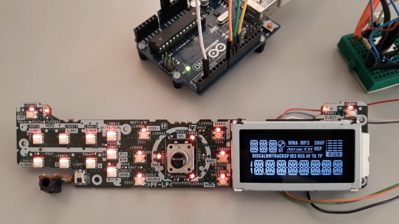
- Sony CDX-A250 Front Panel ใช้ LCD Driver รุ่น LC75826W-0S-E ตาม Service Documentation
- Arduino คุยกับ Panel ผ่าน DATA, CLOCK และ CE
- Current Reference Sketch ใช้ D8, D9 และ D10 ตามลำดับ
- CCB Address ที่ Project ใช้คือ 0x41
- Display Data ครอบคลุม D1–D208 และถูกแบ่งออกเป็น 4 DD Groups
- Data ถูกส่งแบบ LSB First
- Datasheet บอก Electrical Mapping แต่ไม่ได้บอกว่า Sony ต่อแต่ละ Bit ไปเป็น Symbol อะไร
- ผู้สร้างจึงใช้ Push Button + Serial Monitor เปิด Segment ทีละตำแหน่งเพื่อสร้าง Mapping
- Code นี้สร้าง Fixed Pattern เช่น SONY และ CDX-A250 ได้ แต่ยังไม่ใช่ Generic Text Library
- 12 V ใน Project คือ Panel Assembly Supply Path ไม่ใช่แรงดันที่ให้ต่อเข้า LC75826W VDD โดยตรง
ทำไมจอวิทยุรถเก่าต่อ Arduino ไม่ได้ตรง ๆ?
ถ้าเป็น OLED หรือ LCD Module สำหรับ Maker เรามักได้ Controller, Library และคำสั่งระดับสูงอย่าง print() มาให้เรียบร้อย
แต่ Front Panel ของ Sony CDX-A250 ถูกออกแบบมาเป็นส่วนหนึ่งของเครื่องเสียงทั้งระบบ ตัวจอเองเป็น Custom Segment LCD และมี LC75826W เป็น Driver ระหว่าง System Controller กับ LCD Glass
ดังนั้นคำถามไม่ใช่แค่ “ส่งข้อมูลอย่างไร” แต่ต้องตอบด้วยว่า “Bit ไหนทำให้เส้นไหนบนจอสว่าง”
LC75826W ทำหน้าที่อะไร?
Service Documentation ของ Sony ระบุ LCD Driver บน Front Panel เป็น:
LC75826W รับ Serial Data แล้วแปลงข้อมูลนั้น ไปควบคุม Matrix ของ Segment / Common บน LCD
สิ่งสำคัญคือ Driver ตัวนี้ ไม่ได้รับ ASCII Character แบบ Display Module ทั่วไป
Arduino ต้องต่อกับ Sony Panel ตรงไหน?
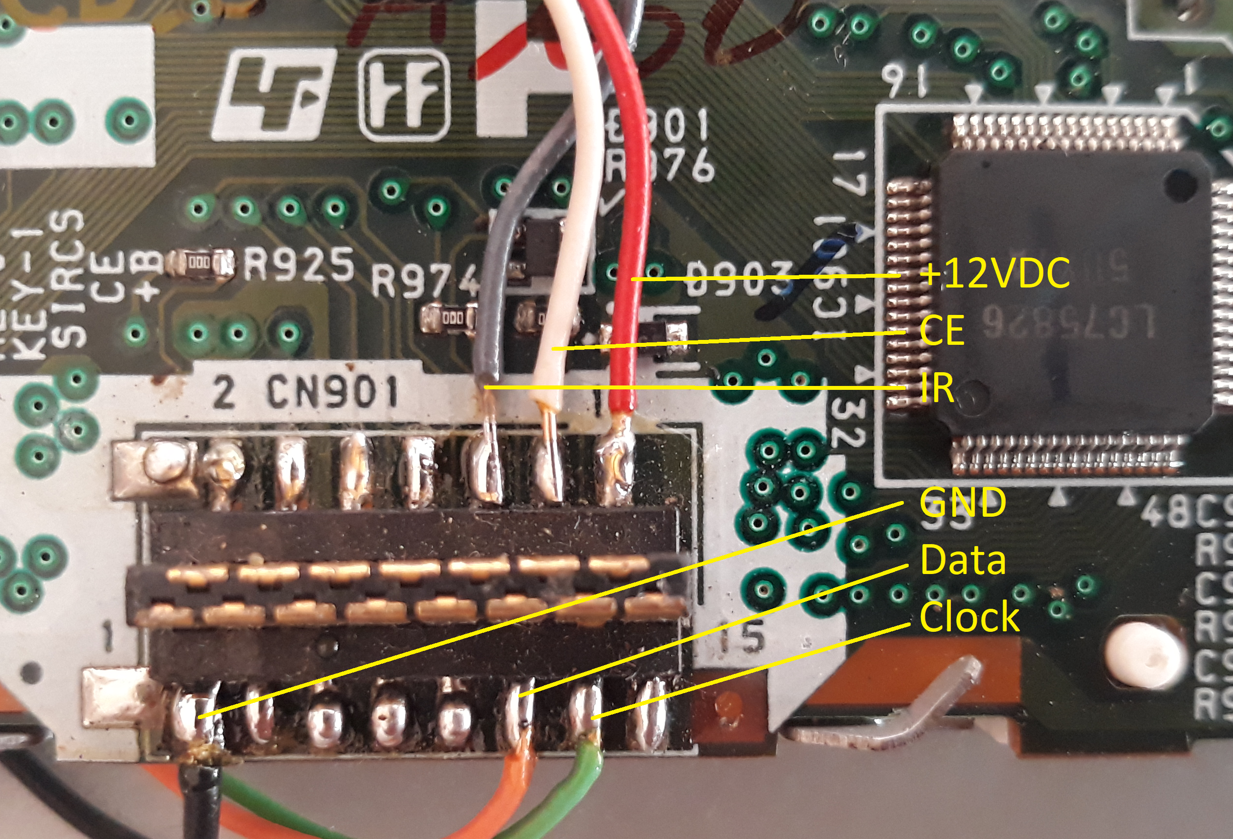
| Arduino | Sony CN901 | Sony Signal | LC75826 Function |
|---|---|---|---|
| D8 | Pin 11 | DATA-LCD | DI |
| D9 | Pin 13 | CLOCK-LCD | CL |
| D10 | Pin 12 | CE-LCD | CE |
| GND | Panel Ground | Common Reference | Ground |
| D2 | Push Button | Segment Test Control | ไม่ใช่ LC75826 Serial Line |
Connector CN901 ยังมี Pin สำคัญอื่น เช่น:
- Pin 1 — D-GND
- Pin 5 — A-GND
- Pin 14 — +B Panel Supply
- Pin 15 — PANEL signal ในระบบ Sony เดิม
Source แนะนำ Series Resistor 1 kΩ บน DATA, CLOCK และ CE เป็น Protection แบบง่ายใน Setup ที่แสดง
Warning: 12 V ใน Project นี้จ่ายให้ Panel ไม่ใช่ LC75826W โดยตรง
Repository ระบุว่า Setup ที่ผู้สร้างทดลอง ใช้ 12 VDC Bench Supply ที่ฝั่ง Front Panel ผ่าน Board-level Supply Path ของ Sony
จุดต่อคือ:
Project จ่ายไฟให้ Panel Assembly ผ่านวงจรบน Board ของ Sony ไม่ได้ Bypass Panel Circuitry เพื่อป้อนไฟ 12 V เข้า VDD ของ IC
ผู้สร้างแนะนำให้ตรวจ Board Revision และใช้ Current-limited Bench Supply ตอน First Power-up
Source ไม่ได้ระบุว่า ควรตั้ง Current Limit เท่าไร ดังนั้นบทความนี้จะไม่สร้างค่าขึ้นเอง
CCB Address 0x41 คือจุดเริ่มต้นของการคุยกับ LC75826W
LC75826 ใช้ Serial Format ที่ Documentation ของ Project เรียกว่า SANYO CCB
Current Arduino Sketch กำหนด:
#define addr 0x41Signal หลักมีเพียง:
- CE — Chip Enable
- CL — Serial Clock
- DI — Serial Data
Sketch จะส่ง Address ก่อน จากนั้นจึงส่ง Display Data ของ Group ที่ต้องการ
Display Data D1–D208 ถูกแบ่งเป็น 4 Group อย่างไร?
หลัง Address Phase LC75826 รับ Display Data เป็น Group และใช้สอง Bit ที่เรียกว่า DD เพื่อบอกว่า Data ชุดนั้นอยู่ช่วงไหน
| DD | Display Data Range |
|---|---|
| 00 | D1–D52 |
| 01 | D53–D104 |
| 10 | D105–D152 |
| 11 | D153–D208 |
Documentation ของ Project ระบุว่า หลัง Address 8 Bit แต่ละ Transfer Group มีข้อมูล 72 Bit
ถ้า LCD ใช้ Data สูงกว่า D152 ต้องส่งครบถึง DD Group `11`
Control Bits P0–P3, DR, DN, FC, OC, SC, BU ทำอะไร?
Group แรกไม่ได้มีแค่ Display Data แต่มี Control Fields สำหรับกำหนดพฤติกรรมของ Driver
| Field | หน้าที่ตาม Documentation ของ Project |
|---|---|
| P0–P3 | เลือก Segment-output / General-purpose-output สำหรับขาที่รองรับสองหน้าที่ |
| DR | เลือก 1/3 bias หรือ 1/2 bias |
| DN | เลือก 200-segment หรือ 208-segment mode |
| FC0–FC2 | Frame-frequency control |
| OC | Internal oscillator / External clock mode |
| SC | Display on / off |
| BU | Normal mode / Power-saving mode |
เวลา Debug จอไม่ขึ้น Control State จึงสำคัญไม่แพ้ Segment Pattern
LSB First: จุดที่อ่าน Binary แล้วพลาดได้ง่าย
Reference Sketch ส่งแต่ละ Byte แบบ:
Function send_char_without() เริ่ม Bitmask ที่:
0b00000001
แล้ว Shift Mask ไปทางซ้าย ทีละตำแหน่ง
นั่นหมายความว่า Literal เช่น:
0B10000000
ไม่ควรถูกตีความว่า Signal บน DI จะออกจากซ้ายไปขวา ตามที่เรามอง Binary Literal ใน Source Code
DD Pattern ใน Reference Sketch
| Final-byte Pattern ใน Source | DD |
|---|---|
0B00000000 |
00 |
0B10000000 |
01 |
0B01000000 |
10 |
0B11000000 |
11 |
ทำไมมี Datasheet แล้ว ยังไม่รู้ว่า Bit ไหนคือตัวไหนบนจอ?
Datasheet ของ LC75826 บอก Electrical Relationship ระหว่าง Segment Outputs, COM Lines และ D1–D208 ได้
ตัวอย่าง:
| Segment Output | COM1 | COM2 | COM3 | COM4 |
|---|---|---|---|---|
| S1/P1 | D1 | D2 | D3 | D4 |
| S13 | D49 | D50 | D51 | D52 |
| S14 | D53 | D54 | D55 | D56 |
| S27 | D105 | D106 | D107 | D108 |
| S39 | D153 | D154 | D155 | D156 |
| S52 / OSCI | D205 | D206 | D207 | D208 |
แต่ Datasheet ไม่รู้ว่า Sony ออกแบบ LCD Glass อย่างไร
ดังนั้นขั้นสุดท้าย ต้องหา Mapping จาก Hardware จริง
เปิด Segment ทีละตัวเพื่อสร้าง Mapping
Reference Sketch มี Routine:
searchOfSegments()segments()
แนวทางคือใช้ Push Button บน D2 เลื่อนไปยัง Test State ถัดไป แล้วดูว่าจอส่วนใดเปลี่ยน
Serial Monitor ใช้:
Workflow ที่ Repository แนะนำ:
- สังเกตว่าจอส่วนไหนเปลี่ยน
- จด Serial Output ของ Step นั้น
- จด DD Block
- จด Byte / Bit Position
- ถ้าสัญลักษณ์ไม่ชัดให้ถ่ายภาพหรือวิดีโอ
- เทียบกลับไปยัง D1–D208
nSeg ใน Reference Routine เป็นเพียง Test-step Counter ไม่ใช่เลข Segment อย่างเป็นทางการจาก Datasheetอีกจุดที่ต้องระวัง: Test Bytes ถูก Complement
ใน Segment Scan Source ส่ง Working Bytes แบบ Invert:
~Aa, ~Ab, ... ~Ah
ถ้าจะ Reproduce Scan เดิม ต้องรักษาพฤติกรรมนี้ไว้ ไม่อย่างนั้นผลที่ได้อาจไม่ตรงกับ Reference
จาก Segment Map ไปสู่คำว่า SONY และ CDX-A250
เมื่อรู้ว่า Bit ไหนควบคุมส่วนไหน ผู้สร้างสามารถสร้าง Pattern สำหรับจอชุดนี้โดยตรง
Current Sketch มี Routine เช่น:
allOFF()allON()msgHiFolks()msgSONY()msgCDX()searchOfSegments()
นี่พิสูจน์ให้เห็นว่า Arduino สามารถควบคุม Fixed Display Pattern บน Front Panel ชุดนี้ได้
lcd.print("HELLO") ได้กับ LCD ทุกตัวทำไม GitHub นี้ไม่ใช่ Generic LC75826 Library?
ผู้สร้างระบุชัดใน README ว่า Repository ตั้งใจเก็บ Working Reference Project ที่เห็นในวิดีโอ
Code จึงถูกผูกกับ:
- Sony CDX-A250 Front Panel
- Segment Mapping ของ LCD Glass ชุดนี้
- Fixed Message Patterns ของ Project นี้
- Board-level Wiring ที่ใช้ในการทดลอง
การเก็บ Code แบบตรงไปตรงมา มีข้อดีตรงที่สามารถย้อนดูได้ว่า Pattern ไหนส่ง Data Byte อะไรจริง
ถ้าจะสร้าง Library ภายหลัง ผู้สร้างแนะนำใน Documentation ว่า อาจแยกเป็น Mapping Table:
แต่ Library แบบนั้น ต้องถือเป็น Implementation ใหม่ และควร Test กับ Hardware อีกครั้ง
ถ้ามี LCD ตัวอื่นที่ใช้ LC75826W ใช้ Code นี้ได้ไหม?
ใช้เป็น Reference ได้ แต่ไม่ควรคาดหวังว่า Upload Code แล้วจออื่นจะแสดงคำว่า SONY ในตำแหน่งถูกต้องทันที
สิ่งที่มีประโยชน์ต่อการ Reuse คือ:
- CCB Communication Concept
- Address / Transfer Structure
- DD Groups
- LSB-first Handling
- Segment-scanning Workflow
- Debugging Strategy
แต่:
จอไม่ขึ้นควร Debug จากอะไร? อย่าเริ่มจากแก้ Pattern ก่อน
Repository แนะนำให้ไล่ระบบ จาก Electrical Layer ขึ้นไปหา Display Data
- ตรวจ Panel Power
- ตรวจ Common Ground
- ตรวจ D8 → DATA-LCD
- ตรวจ D9 → CLOCK-LCD
- ตรวจ D10 → CE-LCD
- ดู CE / CL / DI ด้วย Logic Analyzer หรือ Oscilloscope
- ตรวจว่า Address 0x41 ถูกส่ง
- ตรวจ DD Groups
- ตรวจ Control State
- สุดท้ายจึงตรวจ Segment Pattern
Control State ที่ควรตรวจ
-
SC = 0— Display Enabled -
BU = 0— Normal Mode - INH ต้องไม่ Force Driver / Display ให้อยู่ในสถานะ Inactive
จอขึ้นแค่บางส่วน?
ตรวจว่าได้ส่งครบ:
- DD 00
- DD 01
- DD 10
- DD 11
และตรวจค่า DN ซึ่งเกี่ยวกับ 200 / 208 Segment Mode
LCD กับ Backlight เป็นคนละระบบ
Front Panel มีวงจรอื่น นอกจาก LC75826W รวมถึง Illumination, Panel Controls และ Key-related Circuitry
ดังนั้น:
| อาการ | ไม่ได้หมายความว่า |
|---|---|
| LCD Data ทำงาน แต่ Backlight ไม่ติด | Serial Protocol ผิดเสมอไป |
| Backlight ติด | LC75826 Communication ถูกต้องแล้ว |
เวลา Debug จึงควรแยก:
- Panel Power
- LCD Driver Communication
- Segment Data
- Backlight / Illumination
- Key / Panel Logic
Source Code ที่น่าสนใจ
Repository มี Arduino Sketch ตัวเดียวที่เก็บ Reference Implementation ของ Project ไว้ค่อนข้างตรงกับ Hardware จริง
Pin และ Address
#define VFD_in 8
#define VFD_clk 9
#define VFD_ce 10
#define addr 0x41

#define BUTTON_PIN 2VFD_ เป็น Historical Variable Name ที่ถูกเก็บไว้ใน Source เดิม แต่ Sony Panel ใน Project นี้เป็น LCDLSB-first Transfer
void send_char_without(unsigned char a){
  unsigned char data = 170;
  unsigned char mask = 1;
  data = a;

  for (mask = 0B00000001; mask > 0; mask <<= 1) {
    digitalWrite(VFD_clk, LOW);
    delayMicroseconds(2);

    if (data & mask){
      digitalWrite(VFD_in, HIGH);
    }
    else{
      digitalWrite(VFD_in, LOW);
    }

    digitalWrite(VFD_clk, HIGH);
    delayMicroseconds(2);
  }
}
Push Button สำหรับ Segment Scan
pinMode(BUTTON_PIN, INPUT_PULLUP);

attachInterrupt(
  digitalPinToInterrupt(BUTTON_PIN),
  buttonReleasedInterrupt,
  FALLING
);

Serial.begin(115200);
Segment Scan ใช้ Complemented Bytes
send_char_without(~Aa);
send_char_without(~Ab);
send_char_without(~Ac);
send_char_without(~Ad);
send_char_without(~Ae);
send_char_without(~Af);
send_char_without(~Ag);
send_char_without(~Ah);ดูการ Reverse Engineering จริง
วิดีโอของผู้สร้าง แสดง Process และ Hardware ที่ใช้ในการแกะ Sony CDX-A250 จน Arduino สามารถควบคุม LCD ได้
ข้อจำกัดและจุดที่ต้องรู้ก่อนทำตาม
-
นี่ไม่ใช่ Generic LC75826 Library
Code และ Pattern ถูกสร้างจาก Sony CDX-A250 Front Panel -
จออื่นต้อง Mapping ใหม่
ถึงใช้ LC75826W รุ่นเดียวกัน Visible Segment Mapping ก็อาจไม่เหมือนกัน -
12 V เป็น Panel Supply Path
ไม่ใช่คำสั่งให้ป้อน 12 V เข้า IC VDD -
ต้องตรวจ Board Revision และ CN901 Orientation
ก่อน Apply Power - 1 kΩ Series Resistor ไม่ใช่ Level Shifter
- LSB-first ทำให้ Binary Literal ดูกลับจาก Wire Order
-
nSeg เป็น Test Counter
ไม่ใช่ Official D-number - Segment Scan ใช้ Complemented Bytes
- Backlight และ LCD Interface เป็นคนละ Diagnostic Layer
-
Source ไม่ได้ให้ Current Consumption หรือ Current-limit Setting
จึงไม่ควรสร้างค่าขึ้นเอง
ก่อนจ่ายไฟให้ Front Panel ควรตรวจ Connector Orientation, Board Revision, Short Circuit และ Common Ground พร้อมใช้ Current-limited Bench Supply ตามแนวทางของ Project
อย่านำค่า 12 V จาก Setup นี้ ไปตีความว่าเป็น Supply Voltage ที่ควรต่อเข้าขา VDD ของ LC75826W โดยตรง
FAQ: Sony CDX-A250 LCD และ LC75826W
1. Arduino ควบคุมจอ Sony CDX-A250 ได้จริงไหม?
ได้ใน Project นี้ โดย Arduino ส่ง Serial Data ไปยัง LC75826W บน Front Panel ผ่าน DATA, CLOCK และ CE
2. LCD Driver คือรุ่นอะไร?
Service Documentation ระบุ IC901 เป็น LC75826W-0S-E
3. ใช้ Arduino Pin ไหน?
Reference Sketch ใช้ D8 สำหรับ Data, D9 สำหรับ Clock และ D10 สำหรับ CE
4. Address ของ LC75826W คืออะไร?
Project ใช้ CCB Address 0x41
5. LC75826W รับ ASCII Text ไหม?
ไม่ในรูปแบบที่ Project นี้ใช้ Driver รับ Display-data Bits D1–D208 ไม่ได้ตีความ String โดยตรง
6. ทำไมต้องหา Segment Mapping เอง?
เพราะ Datasheet บอก Electrical Matrix แต่ไม่รู้ว่า Sony ต่อแต่ละ Matrix Position ไปเป็น Stroke หรือ Icon ไหนบน Custom LCD Glass
7. จอมีทั้งหมดกี่ Display-data Bits?
LC75826 Documentation ที่ Project ใช้ ครอบคลุม D1 ถึง D208
8. Data ถูกแบ่งกี่ Group?
4 Group: D1–D52, D53–D104, D105–D152 และ D153–D208
9. Data ส่ง MSB First หรือ LSB First?
Reference Source ส่ง LSB First
10. D2 ใช้ทำอะไร?
ใช้ Push Button สำหรับเลื่อนไปยัง Segment Test State ถัดไป ใน Routine ทำ Mapping
11. Serial Monitor ใช้ความเร็วเท่าไร?
Source ใช้ 115200 baud
12. ทำไมตัวแปรชื่อ VFD ทั้งที่เป็น LCD?
Repository ระบุว่าเป็น Historical Variable Naming ที่ผู้สร้างเก็บไว้จาก Source เดิม Hardware ใน Project นี้เป็น LCD
13. ใช้ Code นี้กับ LC75826W ตัวอื่นได้ไหม?
ใช้เป็น Reference สำหรับ Protocol และ Mapping Workflow ได้ แต่ Visible Segment Mapping ต้องตรวจใหม่ตาม LCD Glass จริง
14. ต้องป้อน 12 V เข้า LC75826W หรือไม่?
ไม่ควรตีความแบบนั้น 12 V ใน Project ถูกใช้กับ Panel Assembly ผ่าน CN901 +B และวงจรบน Sony Panel
15. Repo นี้เป็น Library สำเร็จรูปไหม?
ไม่ ผู้สร้างระบุชัดว่าเป็น Reference Project สำหรับ Sony CDX-A250 ไม่ใช่ Generic LC75826 Library
สรุป: Reverse Engineering จอแบบนี้คือการเชื่อม Datasheet กับ Hardware จริง
สิ่งที่ Project นี้สอนได้ดี คือ Datasheet อย่างเดียว อาจยังไม่พอสำหรับ Custom Hardware
Datasheet ช่วยให้รู้:
- Serial Interface
- Address
- Data Groups
- Control Fields
- Electrical D1–D208 Mapping
แต่สิ่งที่ต้องค้นจาก Hardware จริง คือว่า Sony เอา Matrix เหล่านั้น ไปสร้างตัวอักษรและ Icon แบบไหน
ผู้สร้างจึงไม่ได้เริ่มจาก “เขียน Library ให้สวย” แต่เริ่มจาก “เปิด Bit ทีละตัวแล้วจดสิ่งที่เกิดขึ้น”
เมื่อ Transport ถูกต้อง, Bit Order ถูกต้อง และ Segment Map เริ่มชัด คำว่า SONY หรือ CDX-A250 จึงกลายเป็นเพียงชุด Data Pattern ที่ส่งไปยัง Driver
สำหรับ Maker นี่เป็นตัวอย่าง Reverse Engineering ที่ดีมาก: เริ่มจาก Part Number, Datasheet, Service Manual, Logic Signal แล้วค่อยสร้างความเข้าใจจากของจริงทีละ Layer
โปรเจกต์นี้มีหลาย Layer แนะนำอ่าน Source ต้นฉบับควบคู่กัน
หากจะ Reproduce Hardware ควรอ่านทั้ง Hackaday, GitHub README, Connection Notes, Protocol Notes, Segment Mapping และ Arduino Sketch ก่อนต่อไฟจริง
อ่านบทความ Reverse Engineering บน Hackaday
ดู Source Code และ Documentation บน GitHub
References / แหล่งข้อมูลต้นฉบับ
- Hackaday — Reverse Engineering A Sony Car Stereo LCD
- GitHub — emsyscode/lc75826-sony-cdx-a250
- GitHub Documentation — Connections and Bench Setup
- GitHub Documentation — LC75826 Protocol Notes
- GitHub Documentation — Segment Identification and Mapping
- GitHub Documentation — Manufacturer / Service Manual References
- YouTube — Control a Sony CDX-A250 LCD with Arduino
อยากลอง Reverse Engineering Hardware ด้วย Arduino?
ถ้ากำลังทดลอง Arduino, Development Board, Logic Analyzer, Breadboard, Jumper Wire หรืออุปกรณ์สำหรับ Prototype Electronics สามารถสอบถามทีม Globalbyte เรื่องอุปกรณ์ที่เหมาะกับ Project ได้
งานแบบนี้เหมาะมากกับการฝึกอ่าน Datasheet, ไล่ Signal, ใช้ Serial Monitor และแยกปัญหาระหว่าง Power, Protocol และ Application Logic ทีละ Layer
Repository นี้เป็น Reference Project สำหรับ Sony CDX-A250 Front Panel และผู้สร้างระบุชัดว่าไม่ใช่ Generic LC75826 Library
Segment Mapping ของ Sony LCD Glass เป็น Mapping เฉพาะ Hardware ชุดนี้ LCD รุ่นอื่นที่ใช้ LC75826W อาจมี Visible Segment Mapping ต่างกัน และต้อง Reverse-engineer ใหม่
ตัวแปรใน Source ที่ขึ้นต้นด้วย
VFD_ เป็น Historical Naming แต่ Front Panel ใน Project นี้ใช้ LCD ไม่ควรนำชื่อตัวแปรไปตีความว่า Hardware เป็น VFD Project ใช้ 12 VDC Bench Supply กับ Panel Assembly ผ่าน CN901 Pin 14 (+B) และวงจรบน Sony Panel ไม่ใช่การป้อน 12 V เข้าขา VDD ของ LC75826W โดยตรง
ก่อน Apply Power ควรตรวจ Board Revision, CN901 Orientation, Common Ground, Short Circuit และใช้ Current-limited Bench Supply ตามแนวทางของ Source
Source ไม่ได้ระบุ Current Consumption หรือค่าที่ควรตั้งเป็น Current Limit บทความนี้จึงไม่ได้สร้างค่าดังกล่าวขึ้นเอง
1 kΩ Series Resistor บน DATA / CLOCK / CE เป็น Protection ที่ผู้สร้างใช้ใน Setup นี้ แต่ไม่ใช่สิ่งทดแทน Level Translator หาก Hardware Interface ต้องการ Voltage-level Conversion จริง
Reference Source ส่ง Serial Data แบบ LSB First ดังนั้น Binary Literal ใน C++ ต้องถูกตีความร่วมกับ Wire Transmission Order และไม่ควรอ่านจากซ้ายไปขวา เหมือนลำดับ Bit บนสายโดยตรง
ค่า
nSeg ใน Segment Scan เป็น Test-step Counter ไม่ใช่ D-number อย่างเป็นทางการของ LC75826 Segment Mapping Routine ใช้ Complemented Working Bytes เช่น
~Aa ถึง ~Ah ซึ่งเป็นส่วนหนึ่งของ Reference Behavior Backlight / Illumination, LCD Serial Interface และ Panel / Key Logic เป็นคนละ Diagnostic Layer การทำงานของระบบหนึ่ง ไม่ได้ยืนยันว่าระบบอื่นทำงานถูกต้อง


